
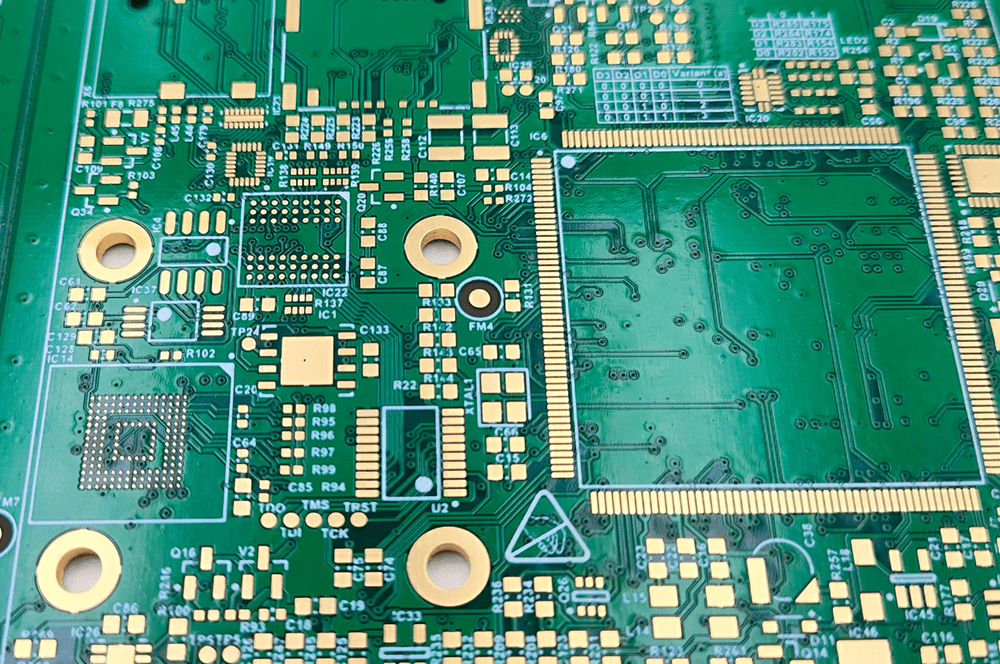
Printed Circuit Boards (PCBs) are like the architects of our electronic world, guiding the flow of electricity in devices ranging from daily used electronic devices such as smartphones and computers, to high-tech electronic applications like medical and aerospace equipment. In short, PCBs navigate electricity and achieve special functions together with electronic components, bringing our electronic devices to life.
PCBs are made with copper wires and dielectric that allow circuits to function and carry out the desired tasks from the PCB designers. In this article, we will closely look at the printed circuit board manufacturing process. We will talk about each step involved in the manufacturing of PCBs, from production files to functional printed circuit boards.
Printed Circuit Board Manufacturing
Printed Circuit Board Manufacturing Process in Simple Steps
Step 1: Design and Output Files for PCB Manufacturer
The first step in the process of manufacturing printed circuit board includes designing and output. Circuit boards need to align seamlessly with the PCB layout designed by engineers using software such as Eagle, OrCAD, Altium Designer, and KiCad. The design is first checked and then approved before manufacturing the PCBs. The design is checked on the industrial parameters and DFM rules. This test is also called design for manufacturer check or DFM. The approved design is then exported in the Gerber format which details the crucial parts of PCB such as apertures, copper trace width and spacing, drill size and position, and more. The first step in the manufacturing of PCBs ensures a smooth file transfer from the designer to the printed circuit board manufacturing companies.
Step 2: Converting Designs to Pattern and Film
Once the designers check the PCB design and approve it for manufacturing, the manufacturers creates a photo film of the design with a special printer known as a plotter. The plotter is a laser jet printer but it is not the ordinary printer that we use in offices and homes. The plotter creates detailed thin images of the PCBs in black ink printed on a plastic sheet. The black indicates the conductive copper parts in the inner layer of the PCBs. The clearer portion of the image is the non-conductive portion of the PCBs. However, for the outer layer of the PCBs the image follows an opposite pattern.
A PCB has two layers – inner and outer. Each layer and solder mask gets its own black and clear film. Meaning the inner layer gets two films one for copper layers and one for the solder mask. In simple words. two layers get four films. Each film contains detailed information on holes, copper wiring, and solder masking. The successful filming of the PCBs takes us to the third step of manufacturing printed circuit boards.
Step 3: Printing the Inner Layers: Copper Placement
In this step, we will use the films created in the last step to map out path for copper on PCB. In short, in step 3, the design patterns from the films are transformed onto copper-clad laminate. The basic structure of PCB is made up of dielectric and copper sheets, and FR-4 CCL is the most widely used one. Now, the excess copper area is removed from the film, and the extra copper will be etched out in the etching process later.
Caution has to be taken while removing copper and placing the film. It is important to maintain cleanliness so as to prevent sand residues from settling and blocking the copper arrangements. It is important to note that dust can cause short circuits and damage the circuits in the PCBs.
Maintaining cleanliness is crucial during PCB construction. The copper-covered laminate undergoes a meticulous cleaning process in a controlled environment to prevent any dust particles from compromising the circuit.
The film with black and clear area is pinned on the board and is exposed to UV light. The UV light hardens the clear area or the area with copper beneath it. The black ink area prevents the surface from hardening. In short, the black ink prevents hardening of the area that will have to be removed in the next step.
Step 4: Eliminating Excess Copper
After exposing the board to the UV light, the process of manufacturing printed circuit boards moves to the next stage: getting rid of unwanted copper. The board is exposed to copper solvent solution that clears away unwanted copper while leaving the desired copper untouched as it is already hardened in the previous step.
Not all copper boards require a similar copper solvent solution for washing away unwanted copper. hard copper boards may need stronger solutions.

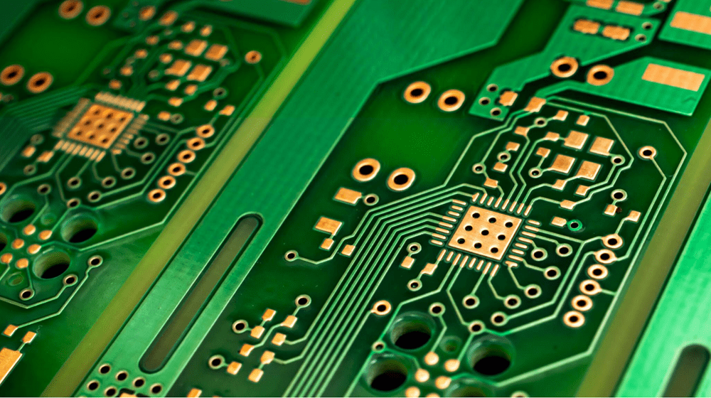
PCB manufacturing-copper trace
Step 5: Aligning Layers and Optical Check
By now, all layers are clean and ready to be aligned. In this step, optical punch, a machine used to punch the holes on the boards, is used to create registration holes on the board. Precise layer alignment is very important in the manufacturing printed circuit board of high layers.
The layers undergo an automatic optical inspection to ensure defect-free panels. A laser sensor scans the layers, comparing the digital image with the original Gerber file. Any inconsistencies are displayed for technician assessment. Once the layers pass inspection, they proceed to the next stages of PCB production.
Step 6: Layering Up and Bonding
In this stage of manufacturing printed circuit boards, the layers are combined to create the final product in two steps – layering and bonding. The first step – layering involves combining the outer layer material consisting of sheets of fiberglass and thin copper foil. After that bonding takes place in which the layers are secured with metal clamps on a heavy steel table. The clamps ensure the layers stay in place. The bonding process is completed through a bonding press computer that controls pressure application, heating, and cooling of the stack.
After the pressing, the technician removes the clamps and removes the pressure plate which gives us a multi-layered PCB securely bonded.
Step 7: Drilling Precision Holes
After lamination in printed circuit board manufacturing, precise holes are drilled into the layered board that we created in the last step. Precise drilling of the holes is important as the holes are the location for components such as copper linking.
The holes are drilled to a smallest diameter like 100 microns. An x-ray locator is used to identify the drill target spots for precise drilling. But before drilling, a board made of buffer material is placed for clean drilling and to prevent any damage to the board because of drilling. The holes are drilled and monitored through a computerized machine.
The drilling takes time as hundreds of holes are to be drilled with each hole having its own dimension and specification. After drilling, a profiling tool removes the extra copper lining the panel edges, exposing the drilled holes that will house vias and mechanical mounting holes.
Step 8: Plating and Copper Deposition
In this step, the PCB is thoroughly cleaned with a chemical solution. The process also involves deposition of a sleek copper layer over the surface of the board. The holes of the board are plated with a new layer of copper while in the interior of the holes are exposed to the base material. The whole process is done through a computerized machine.
Step 9: Outer Layer Imaging
Step 9 is similar to Step 3 for inner layers, the outer layers are imaged with the PCB design. A photoresist layer is applied to the panel in a clean environment to prevent contamination.. UV lights, excluding yellow light, harden the photoresist through black ink transparency secured with pins. A machine removes unhardened resist, and the outer plates are inspected to check the complete removal of the undesired photoresist from the last step.
Step 10: Extra Copper Plating and Tin Protection
In this step, the panel undergoes electroplating to add a thin copper layer, usually 10-20um. Following copper plating, a tin plating process is applied to cover the copper traces. This tin layer protects the copper traces and pads in the next etching stage, and other unprotected areas will be etched out, which are not copper patterns.
Step 11: Copper Etching by Chemcials
Protected by tin, the required copper remains intact while chemical solutions remove excess copper, both exposed and under the remaining resist layer. This step ensures that connections and conducting areas are accurately established, contributing to the PCB’s functionality. This is a critical process in printed circuit board manufacturing since the copper traces carry electricity and achieve electronic functions.
PCB manufacturing-solder mask
Step 12: Solder Mask Printing
After the inner layer copper trace is inspected by AOI, the PCB is cleaned and backed for soldering mask printing. A thin layer of photosensitive solder mask will be printed on the surface of the PCBs, then the PCBs are exposed to UV light to solidate the area which are needed. The unwanted area will be removed by chemical washing.
Step 13: Surface Treament
For prevent the copper pads from oxidation and also increase solderability in PCB assembly process, the PCBs will be coated a thin layer of metal, such as tin, gold, silver., etc. This process results in a surface finish. The most widely used PCB surface finishes are HAL, OSP and ENIG.
Step 14: Component Notation Printing
In this step of PCB printed circuit board manufacturing, the almost finished board is marked with ink-jet printing, conveying essential information about the PCB and all the electronic components. Following this, the board proceeds to the final stage.
Step 15: Circuit Testing
As a crucial measure, a technician conducts circuit tests on the PCB to ensure functionality and adherence to the standard design. Testing is done to detect if there is any open or short circuit. Both the flying probe test and fixture testing are good.
Step 16: Cutting of the Boards into Smaller Panels
In the PCB production process, PCB manufacturers usually produce as big panels, such as 18*24 inches. But this size is too big for delivery and PCB assembly. So we need to cut the big panel into smaller panels as customer’s requirements. The cutting method may involve a router or a v-groove, or even punching with mold. The approach facilitates easy removal of the boards from the panel by the customer or PCB assembly house.
Step 17: Final Quality Inspection
Generally speaking, printed circuit board manufacturing is finished in the above 16 steps, but it is not ready to ship out yet. Final quality inspections will be done by QA departments as below.
- Micro-section checking — for copper plating
- AOI and AVI –for visual defects
- Visual Inspection –for any defects that cannot be detected by machines
- Impedance test –for impedance value check
- Solderability Test –check if PCBs can be soldered well
- Thermal Test –check if PCBs can withstand high temperature in PCB assembly process
- Peel Test (conductor peel strength) –check if there is solder mask peel off issue
- Ionic Contamination Test–check if the PCB has any contamination
- Any other tests customers required
Step 18: Packaging
This is last step, but also important. PCBs will be packed in vacuum packages to avoid humidity and dirt. And PCBs should be packed less than 25pcs per vacuum bag. They should be protected by hard cartons and surrounded by protective material to avoid damage in shipment.
Summary
The above 18 steps are the comprehensive process of printed circuit board manufacturing. Now, we know that the small and green circuit boards are really difficult to process. Lots of equipment and technologies are used in the production process.